TEM/EDS
▍汎銓科技擁有業界最廣泛的TEM佈局,同時提供日系/美系TEM的分析影像滿足客戶所有的需求!汎銓科技TEM設備量充足,提供24小時之材料分析服務!除了提供高解析影像,也大幅提升EDS (Energy-dispersive X-ray spectroscopy 能量分散分析光譜) 分析能力,提供更高品質的 ZC (atomic number contrast) 影像。
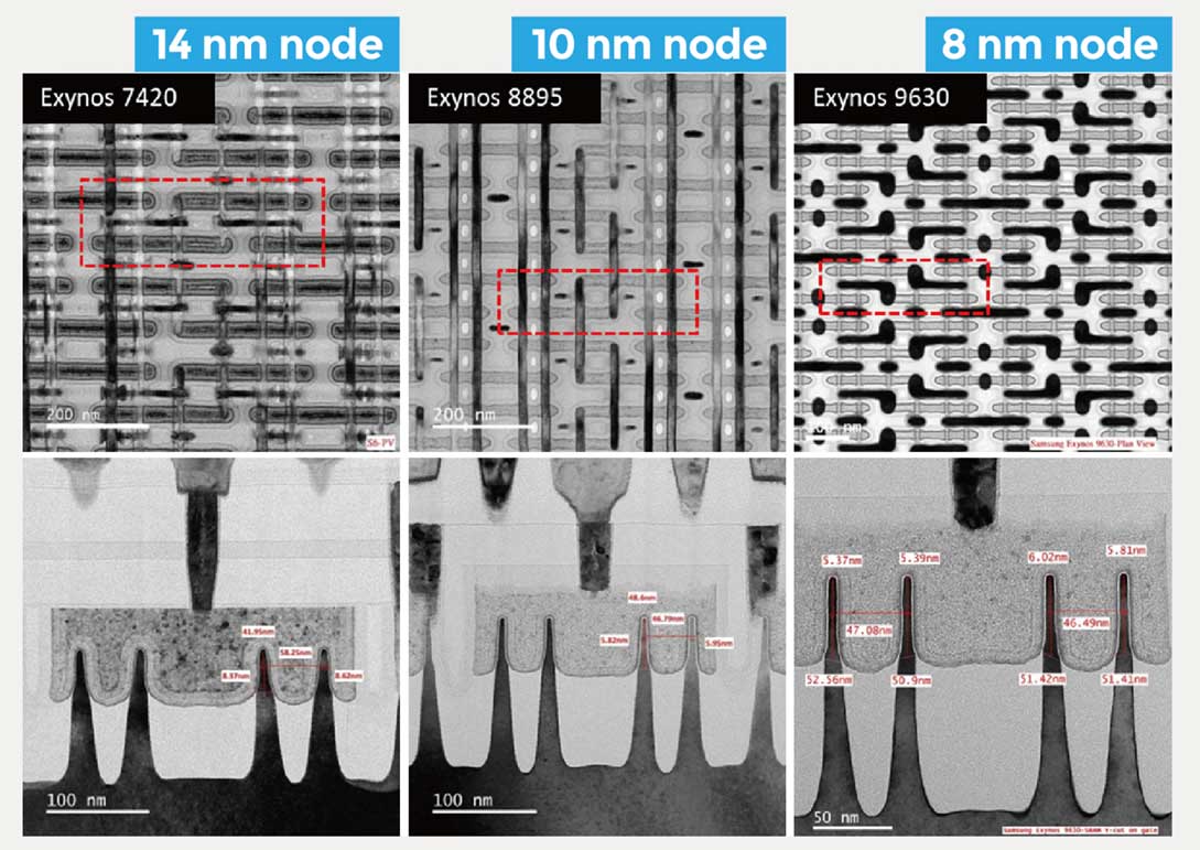
▍TEM images of Samsung application processes
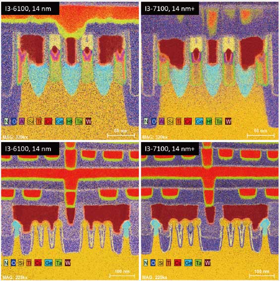
▍TEM images of Samsung application processes
Microstructure analysis: lattice image, IC process monitor, crystal defect observation. Phase identification and composition analysis.
- a TEM inspection of the multi-metal-layer process with Cu dual-damascene structure
- b IC structure observation
- c High resolution TEM with the atomic scale resolution
- d Grain size distribution measurement
- e TEM/EDS analysis for study of Sn whisker growth, the composition distribution of Sn whisker.
TEM inspection of LED MQWs and dislocation distribution.
▍工程聯繫窗口
姚先生 分機6237
E-mail: jack_yao@msscorps.com